Mentors
- M Shreyas Shenoy
- Jalak Kamdar
Members
- Apoorva Agrawal
- Vayun Jain
- Naren G B
Aim
The project aims to demonstrate the functionality and utilization of a FIFO module through Verilog coding and simulation in Xilinx Vivado.
Introduction
FIFO is a crucial data structure used in various digital systems, particularly in data buffering and communication applications.
How does fifo work?
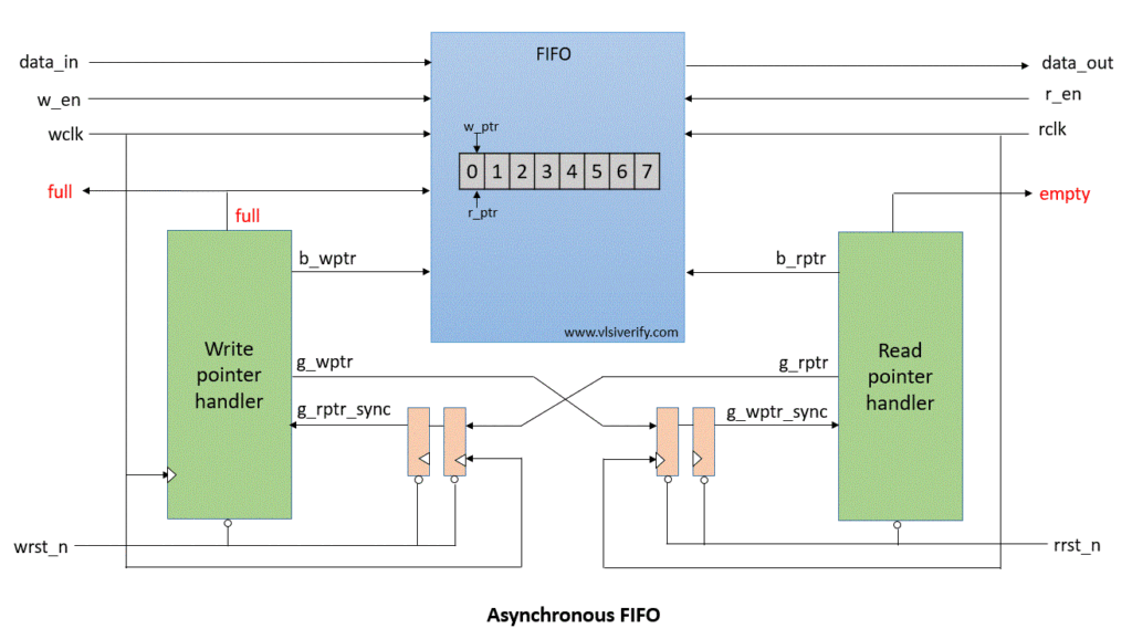
FIFO stands for First In First Out which means data that is written first will be read first. In this project we have implemented an asynchronous fifo. In asynchronous FIFO, data read and write operations use different clock frequencies. Usually, these are used in systems where data has to pass from one clock domain to another which is generally termed as ‘clock domain crossing’. The FIFO design consists of three major components:
###Input and Output Pointers These pointers keep track of the read and write addresses within the FIFO memory. They are responsible for managing the data flow and ensuring proper read and write operations.
###Data Storage Array
The data storage array is a block of memory where the incoming data elements are stored temporarily until they are read out. It operates based on the read and write pointers.
###Control Logic
The control logic module coordinates the overall operation of the FIFO, including managing the pointers, detecting empty and full conditions, and controlling data flow.
##How to use FIFO in clock crossing?
In an asynchronous design, determining empty and full conditions requires crossing clock domains. This invites problems with metastability, where a design might work fine in simulation but not on actual hardware. Indeed, it might work 95% of the time on actual hardware, leaving behind incomprehensible results when it doesn’t work. Fixing these two flags is really the focus of how to build an asynchronous FIFO. This problem is solved by using gray coded read and write pointers and using 2 flip flops as synchronizer to make sure only one bit changes at a time preventing metastability issues.

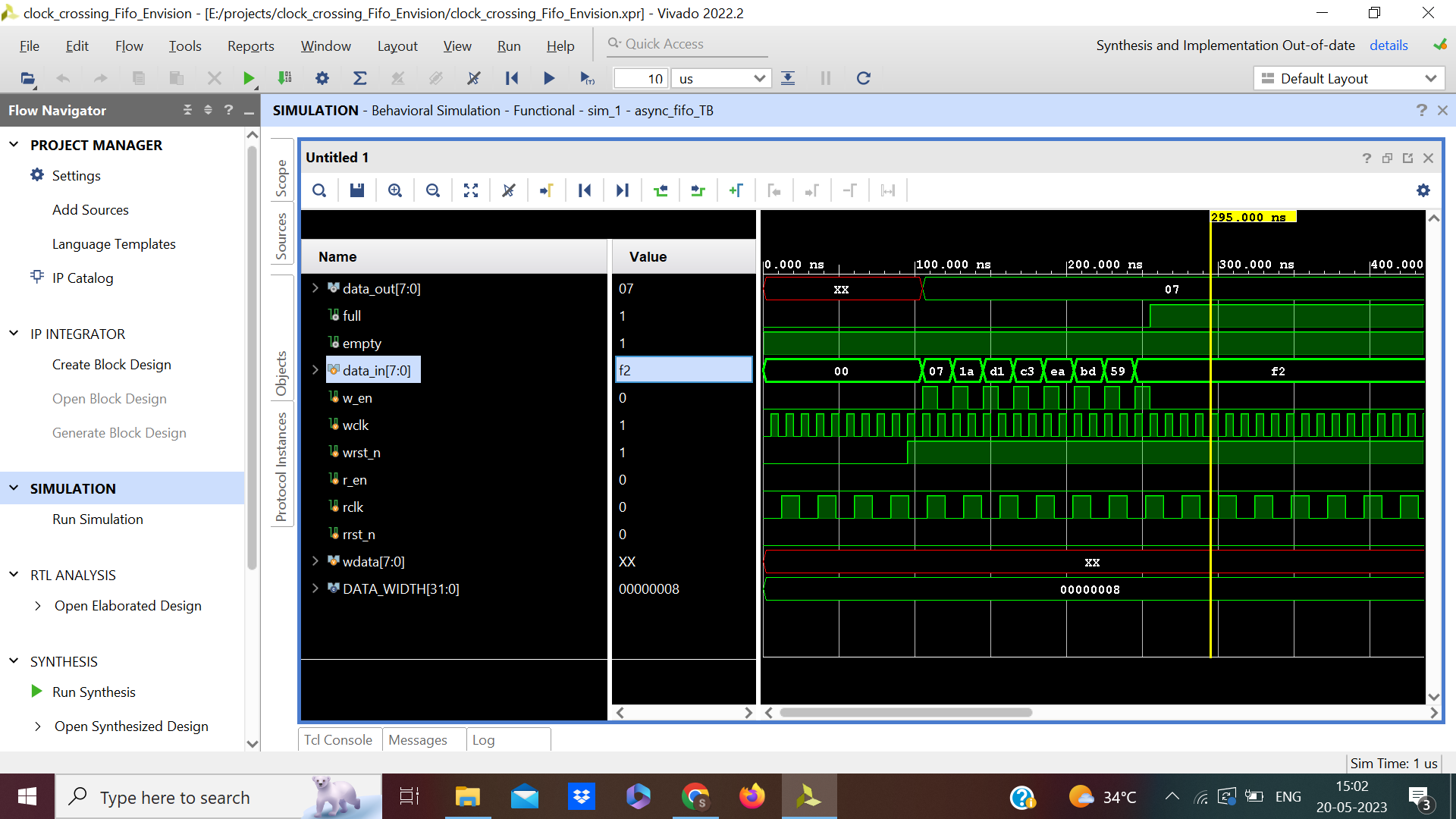
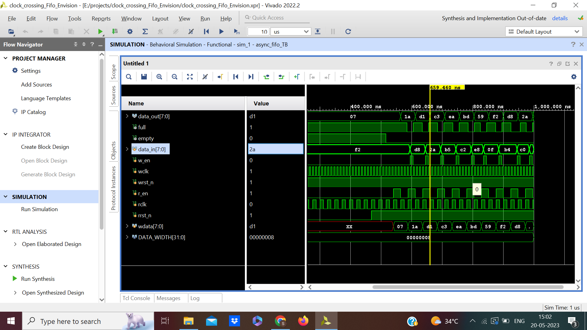
##Results
In this project we were able to obtain the following data in simulation.
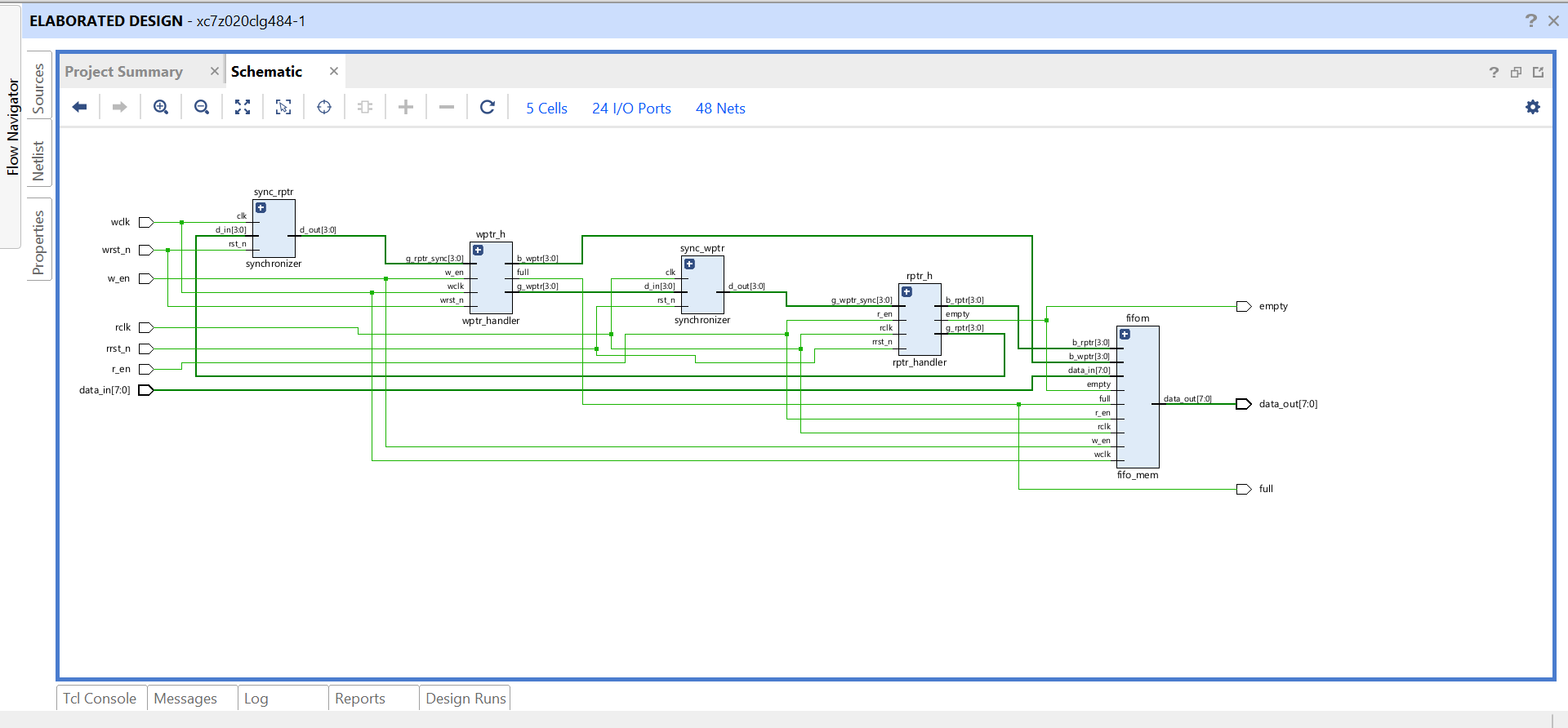
And the following schematic was obtained in Vivado.
Conclusion
- We were able to design the asynchronous fifo and use it for clock crossing domain
- The simulation and schematics were obtained on Vivado and verified.
Future prospects
Implement the code on an FPGA
References
1.
- https://zipcpu.com/blog/2018/07/06/afifo.html
- http://www.sunburst-design.com/papers/CummingsSNUG2002SJ_FIFO1.pdf