Guides
- Prof. M S Bhat, National Institute of Technology Karnataka
- Aditya Kulkarni
Team Members
- Sahith S R
- Iteesha V A
- A Shrikant
Objectives
- Analyzing the Lower metal layers of the On-Chip interconnects using the proposed model.
- Calculating the efficiency and accuracy of the proposed model against the foundry parameters.
- Designing a GUI for displaying the results acquired from the model for any interconnect lengths.
Introduction and Methodology
The advent of shrinking technology nodes in Integrated Circuit (IC) fabrication has led to the development of multi-layer metal connections to support a high density of transistors in a small chip area. From earlier foundry fabrication techniques, modern foundries support greater than 6 metal layers. On-chip interconnects consist of these metals in each layer. Metal lines which connect transistor devices in the same layer are defined as intra-planar interconnects.
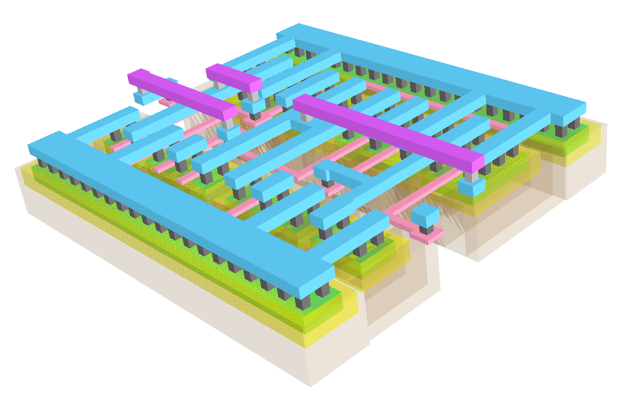
This figure shows the metal density in the 3D view of a simple 2-input XOR gate. The blue lines indicate the lowest metal layer, M1, and the purple lines represent the next metal layer,M2. The high density metal connections in the lower metal region make the non-ideal interactions of the metal layers more significant and therefore, there is a need to model these non-idealities to better understand the on-chip behaviour of these high density circuits. This project aims to model the non-idealities present in the lowest metal layer, M1.
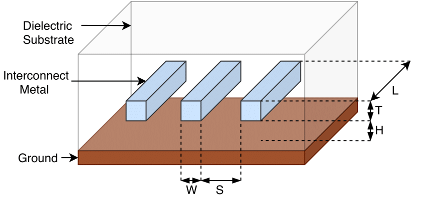
The lower metal layer wires were modelled using the proposed pi-model RLC network. The RLC values of the pi-network was carefully chosen to match the actual characteristics of the wire under test. The lengths of the interconnects was chosen as the parameter of interest.
So the model’s accuracy was analyzed wrt. different interconnect lenghts. The other parameters like other dimensions of the wire, nature of materials and media were taken to be fixed. The actual foundry parameters and equivalently, the actual circuit behaviour was obtained using a simualtion software ‘Electric Binary’, which has ‘LT Spice IV’ on background, a primary tool for circuit simulation.
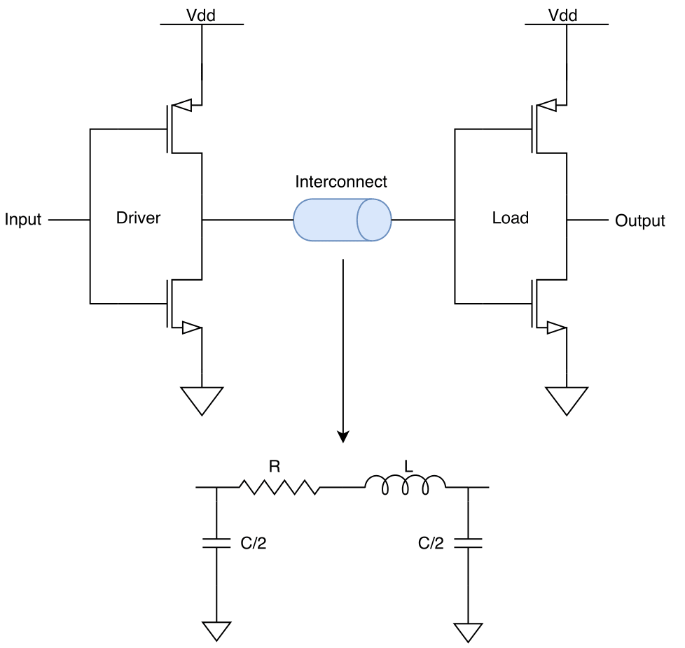
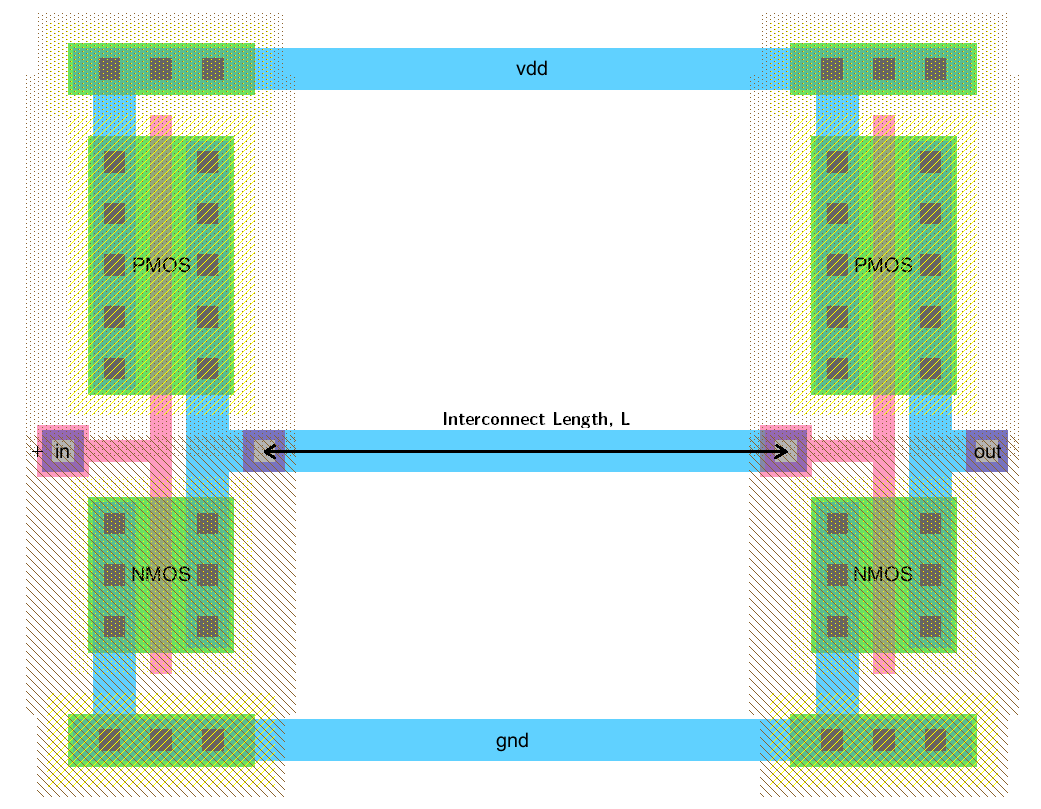
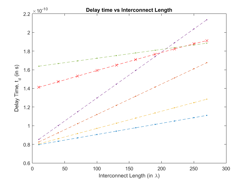
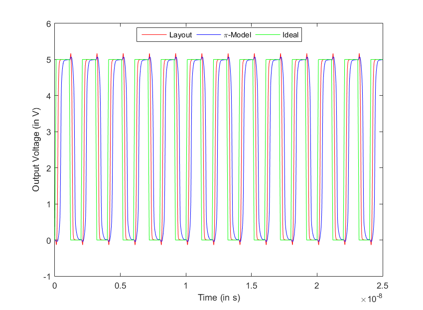
The transcient analysis on LT Spice was used as the main tool for the analysis. The model was first put on simulation using a driver-load inverter pair(CMOS inverter pair) and the time delay(or phase delay equivalently) between the waveforms resulted from using the proposed model and the actual foundry circuits. The model was put up between the inverters for the analysis. Various interconnect lenghts were used and the corresponding delays were plotted. The result of the model was a schematic file and that of the foundry values is given as the layout file.
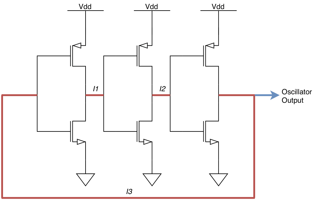
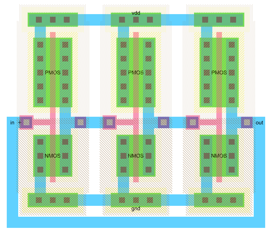
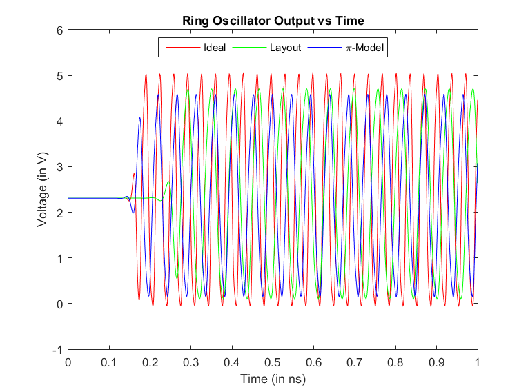
Similarly, the analysis was repeated on a 3 stage CMOS Ring Oscillator circuit and the results were analyzed. In case of the Ring Oscillator, the accuracy is computed in terms of the frequency of oscillations generated by the schematic circuit was compared with the layout.
Results
In case of the driver-load inverter pair, various plots of td vs interconnect length were obtained on different T/H ratios(thickness to height) and found that model provided fairly accurate results for T/H close to 1.
In case of the 3 stage CMOS Ring OScillator, the model presented fairly accurate results. The output frequency produced by the circuit with the model was within a range of 20% from the layout circuit(with foundry parameters).
Applications
The modelling of the interconnects using a RLC network can be very useful for simulation softwares to generate accurate results at a higher frequencies with a higher efficiency (in terms of complexity of computation). So one of the main application of this project is to understand and predict the behaviour of on-chip interconnects at high frequencies and suitably study them.
Acknowledgements
We would like to acknowledgea and appreciate the help and support given by both of our guides Aditya Kulkarni and Prof. M S Bhat and we thank IEEE-NITK Student Branch for supporting this project.
Note: The final presentaion video can be found here and the link to the slides can be found here