Mentors
- Akash S Bharadwaj
- Achintya
- Sankarsh
Members
- Anirudh Singh Solanki
- Apurva S
- K A Gaganashree
Introduction
Microprocessors and Microcontrollers are generally designed in the vicinity of two main computer architectures: Complex Instruction Set Computing i.e. CISC architecture and Reduced Instruction Set Computing i.e. The main idea of CISC is that a single instruction will do all loading, evaluating, and storing operations just like a multiplication command will do stuff like loading data, evaluating, and storing it, hence it’s complex. Thus causing them to have varying execution time and lengths thereby authoritatively mandating an intricate Control Unit, which inhabits an immensely existent region on the chip.
Compared with their CISC analogue, RISC processors typically support a minuscule set of instructions. A display that juxtaposes RISC processor with CISC processor, the number of instructions in a RISC Processor is low while the number of general purpose registers, addressing modes, fixed instruction length and load-store architecture is more this in turn facilitates the execution of instructions to be carried out in a short time thus achieving higher overall performance .Currently, the efficacy of the RISC processors is generally accepted to be greater than that of their CISC counterparts. Before their execution the instructions are translated into RISC instructions in even the most popular CISC processors. The attributes mentioned above accentuate the design strength of RISC in the market for embedded systems known as “system-on-a-chip (SoC)”. The premier micro processors exhibiting reduced instruction set are SPARC, ARM, MIPS and IBM’s PowerPC. RISC processors typically have load store architecture. This denotes there are two instructions for accessing memory which are a load instruction set to load data from the memory and store instruction set to Write Back (WB) the data into memory without any instructions
Objective
To generate a full GDSII from a RTL netlist for a fully working and optimized RISC microprocessor from scratch using openLane.
MIPS Instruction Set Architecture:
Instructions are encoded as 32-bit instruction words.The instruction set can be categorized under three classifications in the MIPS ISA, these are: Register type (R), Immediate type (I) and Jump type (J).
The following table demonstrates the three formats used for MIPS core instruction set architecture.
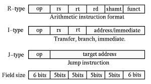
R-format Instructions:

Instruction Fields -op : operation code (opcode) -rs : first source register number -rt : second source register number -rd : destination register number -shamt : shift amount (00000 for now) -funct : function code (extends opcode)
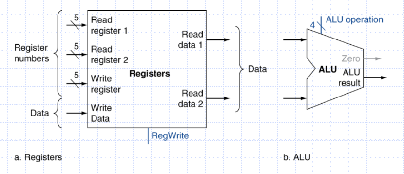
In R-format instructions the data is read from two register operands (rs & rt) .These instructions are used to perform arithmetic and logical operations and write back the result into the register stored in rd.
Immediate (I) format:

Types of instructions: load, store, addi
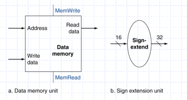
Immediate arithmetic and load/store instructions -rt : destination or source register number -Constant: -2 ^15 to +2 ^15 -Address: offset added to base address in rs
Encode full address in instruction

(Pseudo)Direct jump addressing Target address = PC 31…28 : (address × 4)
Branch Addressing
Branch instructions specify Opcode, two registers, target address. Most branch targets are near branch.

PC relative addressing Target address = PC + offset × 4 PC already incremented by 4 by this time
Instruction execution:
Microprocessor without Interlocked Pipeline Stages (MIPS) is a RISC (Reduced Instruction Set Computing) architecture.Pipelining means several operations in a single data path at the same instant. Pipelined MIPS has five stages which are IF, ID, EX, MEM and WB.
MIPS PIPELINE
Five stages, one step per stage
- IF: Instruction fetch from memory
- ID/RF: Instruction decode & register read
- EX/EA: Execute operation or calculate address
- MEM: Access memory operand
- WB: Write result back to register
Pipelining is used to enhance the capabilities of the RISC processor which is the reason for its utilization in this type of computer architecture. A multi cycle CPU comprises countless tasks. So if one task occurs, rather than waiting for the process to finish, at the same time another task is initiated in the same data path simultaneously without interfering with the previous task. The process is thus divided into different pipelined stages. Following every clock a new operation is loaded into the program counter (PC) in the pipeline stage to which the process is being fed to. The triggering is done without causing any interruptions to the past process. This makes simultaneous utilization of all stages in the data path possible. This thus can increment the throughput of MIPS.
CPU Overview
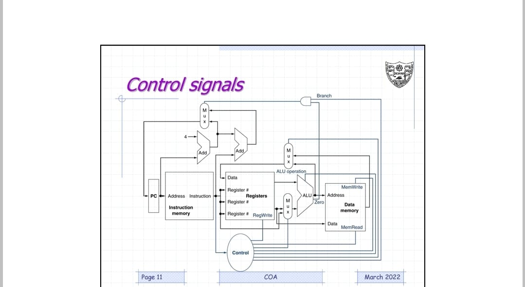
The control unit tells the datapath what to do, based on the instruction that’s currently being executed. Our processor has ten control signals that regulate the datapath.The control signals can be generated by a combinational circuit with the instruction’s 32-bit binary encoding as input.
Datapath Design
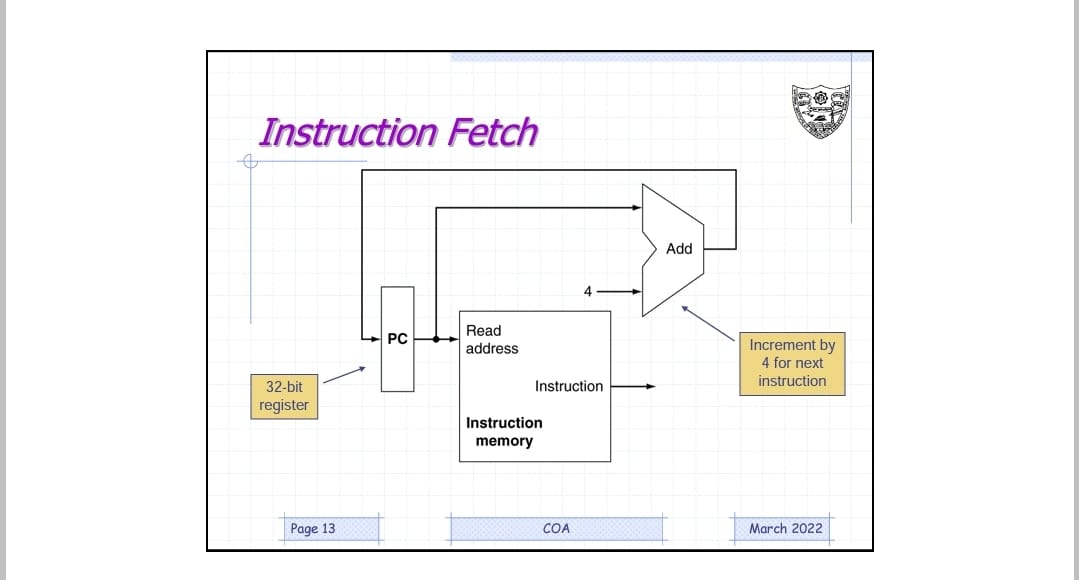
In this stage, the instruction memory receives the address of 32 bit instruction given by the Program Counter(PC). Using the address the instruction is fetched from the instruction memory.
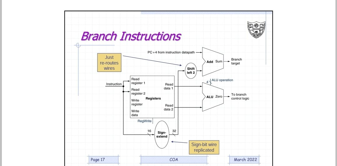
In branch type instructions when the instructions are decoded. We need an alu unit to compare the value in both the registers(rs and rt). for example in beq instruction if the value in both the registers are same then a zero flag in alu unit is triggered and program counter (PC) will branch to that address mentioned in executing instruction (calculated by sigh extending the 16 bit address/ constant)
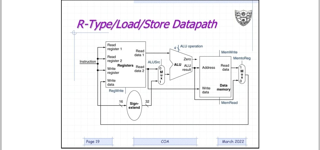
The two elements needed to implement R-format ALU operations are the register file and the ALU. The register file contains all the registers and has two read ports and one write port. The register file always outputs the contents of the registers corresponding to the Read register inputs on the outputs; no other control inputs are needed. In contrast, a register write must be explicitly indicated by asserting the write control signal. The RISC-V load register and store register instructions, which have the general form ld x1, offset(x2) or sd x1, offset(x2). These instructions compute a memory address by adding the base register, which is x2, to the 12-bit signed offset field contained in the instruction. If the instruction is a store, the value to be stored must also be read from the register file where it resides in x1. If the instruction is a load, the value read from memory must be written into the register file in the specified register, which is x1.
ALU Control
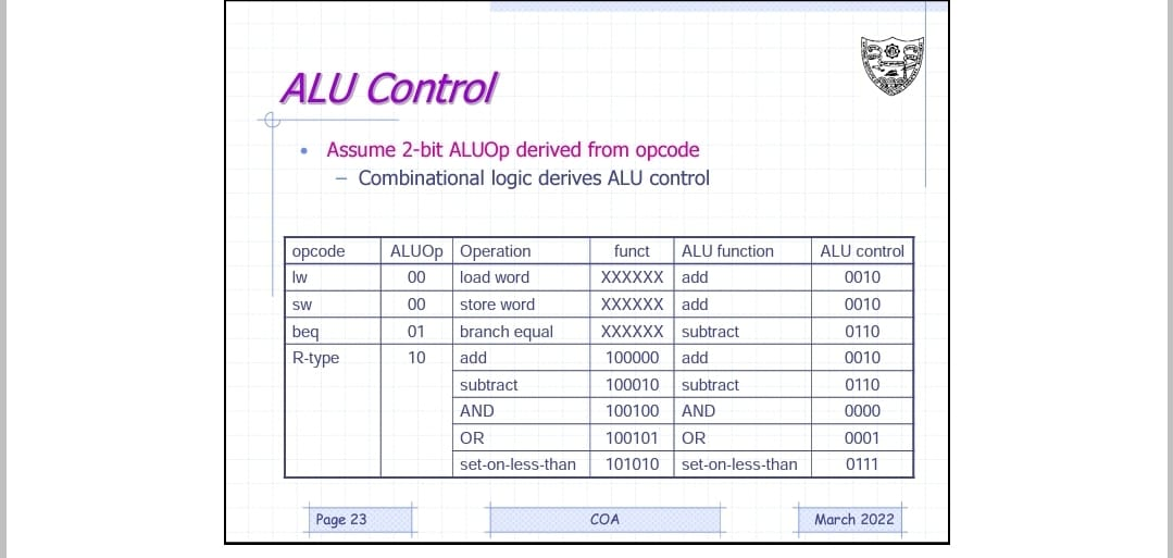
Alu control takes in function code and shift amount as input and a combinational logic derives alu control signals to the ALU unit. These alu control signals decides which alu operation has to be performed while taking in what type of instruction is given
Full Datapath
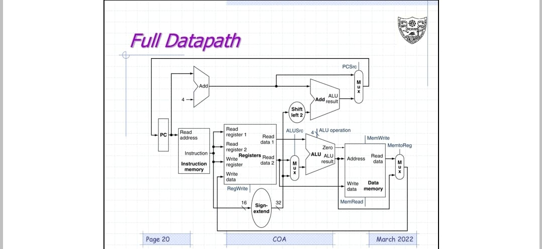
Here all stages discussed above are linked together.
Datapath with Control
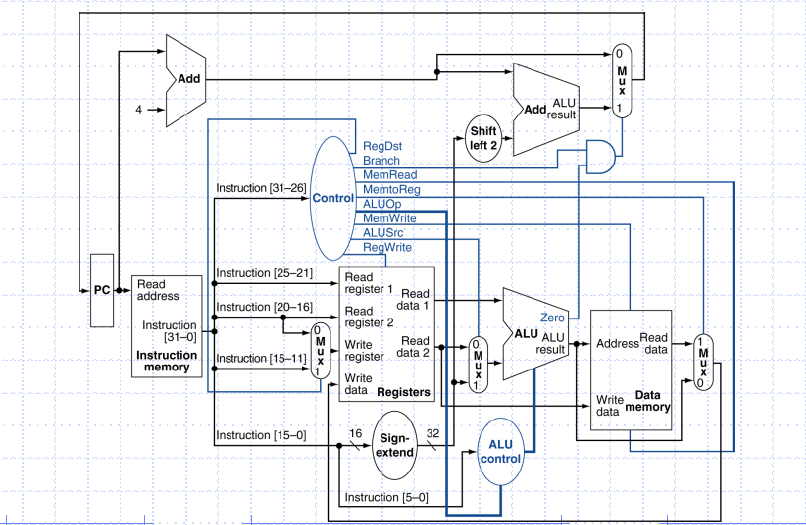
Processor design:
MIPS processor is executed utilizing five pipeline stages, which are Instruction Fetch (IF), Instruction Decode (ID), Execution Stage (EX), Memory access (MEM) and Write Back (WB). This isolation of stages is achieved by special registers known as pipeline registers. The aim of These registers are to isolate the stages of the instructions so that there is no inadmissible information because of various directions being executed all the while. They are named in the middle of each of these: IF/ID Register, ID/EX Register, EX/MEM Register and MEM/WB Register. The data path demonstrated in above figure is that of the MIPS pipelined processor.
Physical design preview
Physical design of the processor can be obtained using a tool called OpenLane. OpenLane is an automated RTL to GDSII flow based on several components including OpenROAD, Yosys, Magic, Netgen, CVC, SPEF-Extractor, CU-GR, Klayout and a number of custom scripts for design exploration and optimization. The flow performs full ASIC implementation steps from RTL all the way down to GDSII.
This tool is used for Macro Hardening and SoC integration
Macro Hardening is converting RTL Design to corresponding physical views such as GDS view
and SoC integration is Adding IO pads, floor planning the chip using other hardened macros.
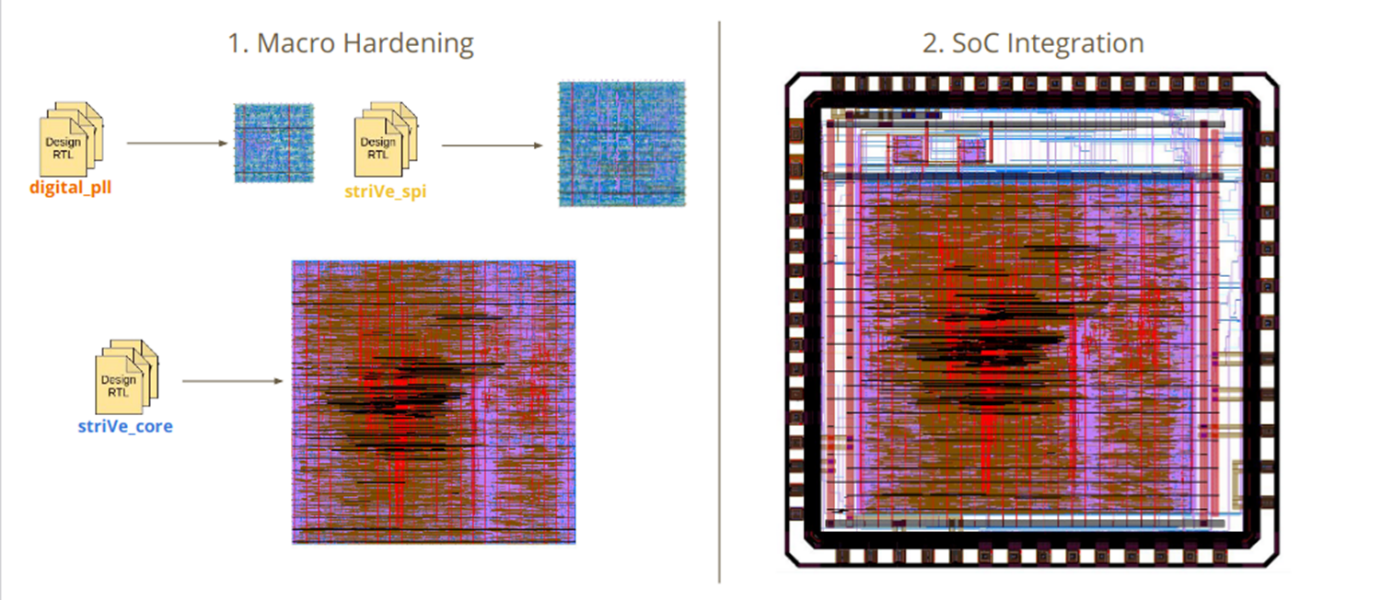
This is the OpenLane Macro Hardening basic flow
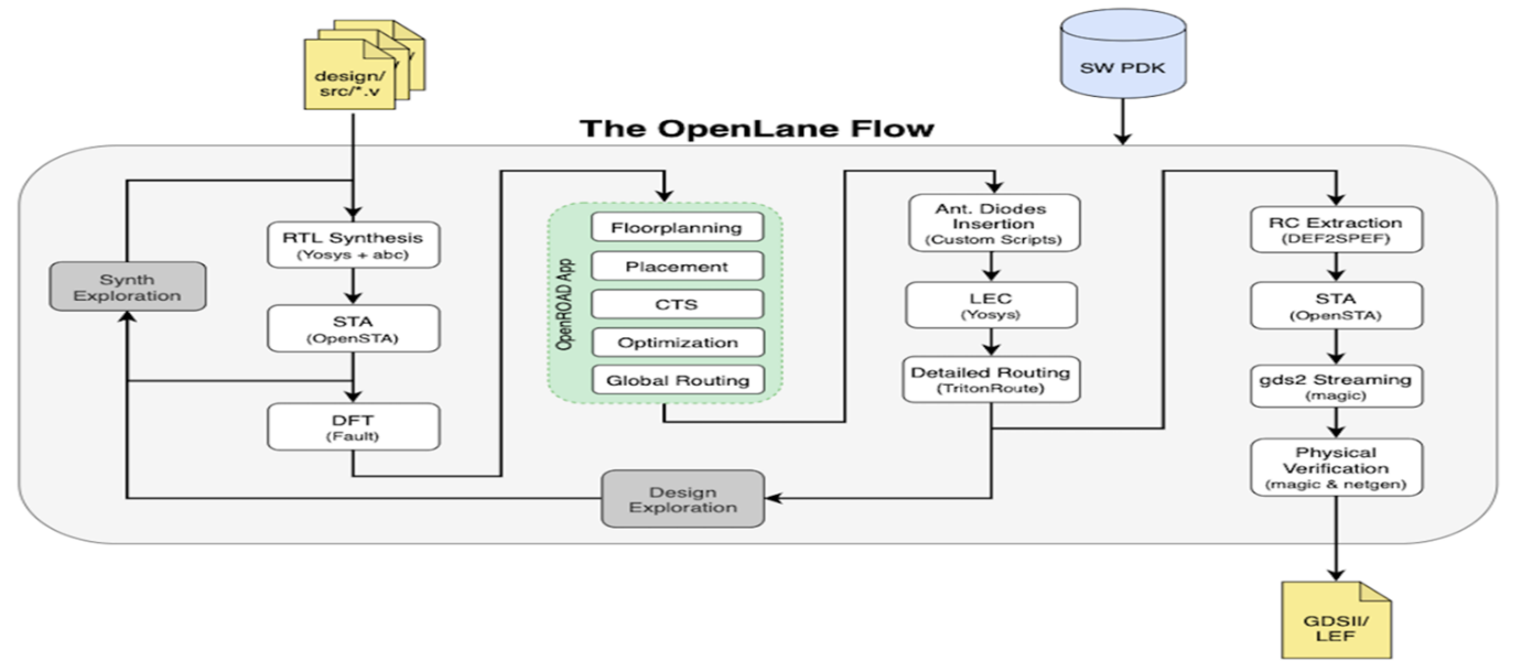 OpenLane flow consists of several stages. By default all flow steps are run in sequence. Each stage may consist of multiple sub-stages. OpenLane can also be run interactively as shown here.
1. Synthesis
i. yosys - Performs RTL synthesis
ii. abc - Performs technology mapping
iii. OpenSTA - Performs static timing analysis on the resulting netlist to generate timing reports
2. Floorplan and PDN
i. init_fp - Defines the core area for the macro as well as the rows (used for placement) and the tracks (used for routing)
ii. ioplacer - Places the macro input and output ports
iii. pdn - Generates the power distribution network
iv. tapcell - Inserts welltap and decap cells in the floorplan
3. Placement
i. RePLace - Performs global placement
ii. Resizer - Performs optional optimizations on the design
iii. OpenDP - Perfroms detailed placement to legalize the globally placed components
4. CTS
i. TritonCTS - Synthesizes the clock distribution network (the clock tree)
5. Routing
i. FastRoute - Performs global routing to generate a guide file for the detailed router
ii. CU-GR - Another option for performing global routing.
iii. TritonRoute - Performs detailed routing
iv. SPEF-Extractor - Performs SPEF extraction
6. GDSII Generation
i. Magic - Streams out the final GDSII layout file from the routed def
ii. Klayout - Streams out the final GDSII layout file from the routed def as a back-up
7. Checks
i. Magic - Performs DRC Checks & Antenna Checks
ii. Klayout - Performs DRC Checks
iii. Netgen - Performs LVS Checks
iv. CVC - Performs Circuit Validity Check
Before running the whole design we are expected to perform synthesis exploration of the design. Which is the process of getting different netists using different synthesis strategies.
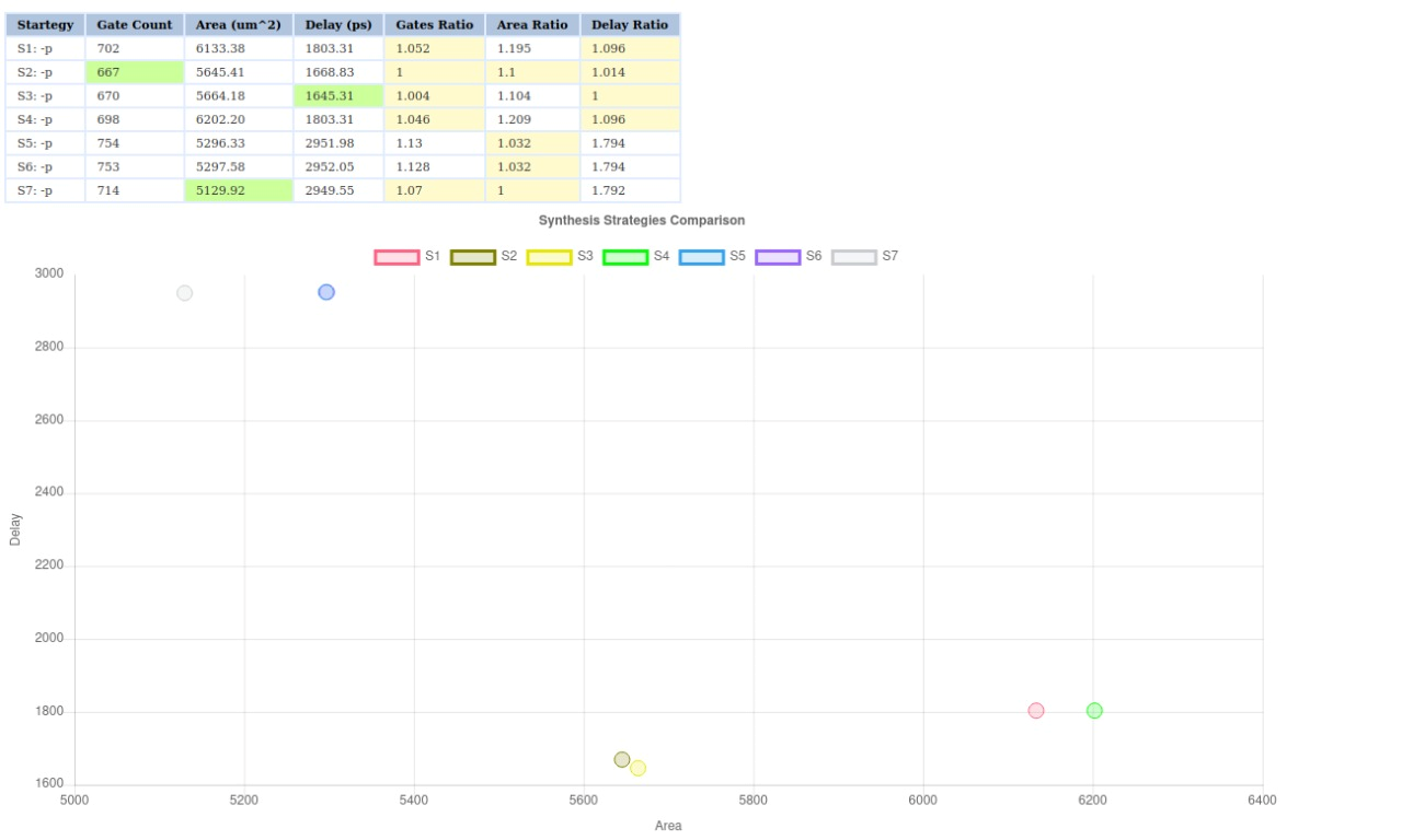
The above figure shows 7 different strategies which one can follow to choose the most suitable design.The plot gives information about the delay and area of the design. One should aim to select the strategy with least area and delay. After choosing the strategy best suited, we need to then add it in the config.tcl file. Finally, we can run our design and obtained the GDSII view.
Results and Discussion
Successfully implemented all the 5 pipelining stages in verilog
Conclusions and future work
When we ran the design on OpenLane, a few modules gave errors. After sorting them, we will be implementing branch prediction and feed forwarding.