Mentors
- K A Gaganashree
- Meghna Uppuluri
Members
- M N Vishnu
- Sreehari Krishnan
- Alex Moby Philp
- Siddharth Vydyula
- Launnish
Aim
This project aims to interface different Peripherals, Memory integrated with RISC-V(Reduced Instruction Set Computer) processor and successfully implement it on FPGA.
Introduction
SoC is an acronym for System on Chip is an IC (Integrated Circuit) which integrates all the components into a single chip and consists of a microprocessor and its subsystem customized to the desired functionality. Modern-day SoC has fundamentally evolved over the years and is now traditionally deployed in communications, data storage, and high-tech computing domains.
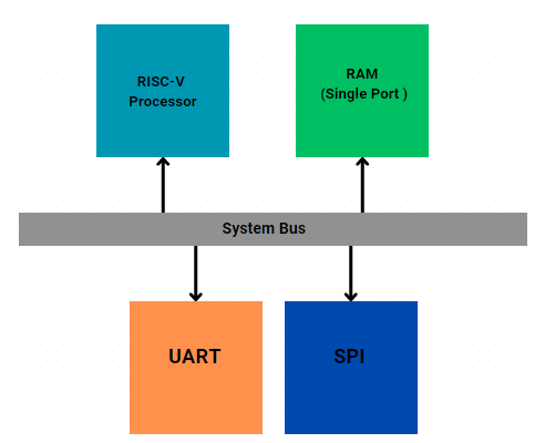
About RISC-V Processor
FemtoRV is a minimalistic RISC-V design, with easy-to-read Verilog sources directly written from the RISC-V specification. The most elementary version (quark), an RV32I core, weights 400 lines of VERILOG (documented version), and 100 lines if you remove the comments. We will be using FemtoRV32 quark version for our SoC.
Peripherals
UART
UART(Universal Asynchronous Receiver Transmitter)
- An interface that sends out data usually byte at a time over a single wire.
- Data transfer is independant of clock pulse hence asynchronous
- UARTs can operate in either Half-Duplex(two transmitters sharing a line) or Full-Duplex(two transmitters each with their own line).
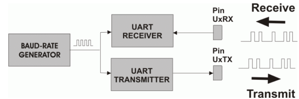 Image courtesy : link
Several Parameters that can be set by user
- Baud Rate (bits transmitted per second)
- Number of Data bits
- Parity Bit
- Stop bits
As mentioned this interface does not have a clock, the data must be sampled to recover it correctly. It needs to be sampled at least eight times faster than the rate of the data bits. </br> This means for an 115200 baud UART, the data needs to be sampled at least at 921.6 KHz (115200 * 8 bits).
UART communication
- Transmitter
- Receiver
Transmitter ( tx )
It transmits the data serially 8 bits per second. The signals used in the transmitter.
i_clkis used for the clock signal.- Transmits the data only when the
i_wrsignal is asserted. Else transmits high signal. i_datastores the start bit ( zero ) with the data bits to be transmitted.o_busysignal indicates whether the transmitter is transmitting the data or not.- The single bit output of the transmitter is given by
o_uart_txsignal.
We have 4 registers
state,baud_counter,local_data,baud_stb, for storing the state of the FSM, the clock cycles, the data bits with start and stop bits, and a flag (for indicating the readiness to transmit next bit i.e., transmits next bit if it is high) respectively.
There are 10 states in our FSM
BIT_ZERO,BIT_ONE,BIT_TWO,BIT_THREE,BIT_FOUR,BIT_SIX,BIT_SEVENare 8 states each for 8 different bits.LASTfor last bit in transmition.IDLEwhen the transmittion isn’t taking place.
Working
- This module takes
i_clk,i_data,i_wras inputs and outputso_busy,o_uart_tx. Initially the state is madeIDLEando_busywill be low, since the transmission is not started. We have 3 always block which are triggered for each positivei_clkedge. - The first block is the state machine. Initially transmission starts when the
i_wris high ando_busyis low,o_busyis asserted and state is assigned asSTARTas soon as the transmission starts. - When the
baud_stbis high is when state chnages or not. Ifstateis atIDLEthen it remains atIDLEando_busybecomes low , otherwise it leads to incrementation of state ando_busybecomes high. - The
baud_counteracts as a decremental counter that keeps track of number of cycles between each bit. - When state changes from
BIT_SEVENtoLAST, all bits have been transferred.
Receiver ( rx )
It receives data bit by bit at the rate of 8 bits per second.
i_clkis used for the clock signal.i_rx_datais bitwise input data signal included with start and stop bits.o_wris asserted when the data ino_datais ready to be read.o_datais an output register to output the recived data.
We have 5 registers
STATE,baud_count,zero_baud,ck_uart,q_uart. For storing fsm state, clock cycles, flag to start next state. where we useck_uartto induce delay.
There are 10 states in our FSM
BIT_ZERO,BIT_ONE,BIT_TWO,BIT_THREE,BIT_FOUR,BIT_FIVE,BIT_SIX,BIT_SEVENare 8 states for different bits.IDLEwhen there’s no receiving taking place,STOP_BITto terminate the receiving after getting all 8 bits.
Working
- This module takes
clk,i_rx_dataas inputs and outputso_wr,o_data. Initially the state is madeIDLEando_data,o_wrwill be low, since the receiving is not started. We have 4 always block which are triggered for each positiveclkedge. - When
ck_uartbecomes low, it means start bit is detected, state changes fromIDLEtoBIT_ZEROandbaud_countis initilized. - The
baud_countacts as a decremental counter that keeps track of number of cycles between each bit. When thebaud_countreaches zero thenzero_baudflag is set high which increments the state. When state changes fromBIT_SEVENtoSTOP_BIT, all bits have been received and the receiving process stops.
SPI
SPI is a synchronous, full duplex main-subnode-based interface. The data from the main or the subnode is synchronized on the rising or falling clock edge. Both main and subnode can transmit data at the same time. The SPI interface can be either 3-wire or 4-wire.
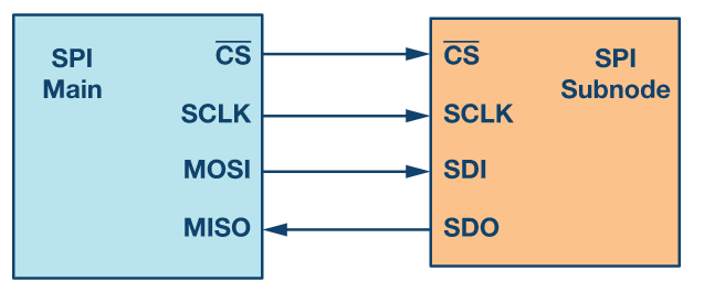 Image courtesy: Analog Devices
Memory
Integrating a Synchronous Dynamic Random Access Memory (SDRAM) with a RISC-V processor typically involves designing a memory controller that interfaces with the SDRAM and communicates with the processor through a bus interface. The memory controller manages the flow of data between the processor and the SDRAM, handling tasks such as address decoding, read and write operations, and refresh cycles.
Wishbone
The WISHBONE System-on-Chip (SoC) Interconnection Architecture for Portable IP Cores is a flexible design methodology for use with semiconductor IP cores. Its purpose is to foster design reuse by alleviating System-on-Chip integration problems. This is accomplished by creating a common interface between IP cores. This improves the portability and reliability of the system, and results in faster time-to-market for the end use.